
Dowa has been granted a patent for a semiconductor light-emitting device featuring a reflective metal layer, an InGaAsP-based semiconductor laminate, and an n-type InGaAs contact layer. The device emits light with a center wavelength between 1000 to 2200 nm and has a total laminate thickness of 2 to 8 µm. GlobalData’s report on Dowa gives a 360-degree view of the company including its patenting strategy. Buy the report here.
Smarter leaders trust GlobalData
Discover B2B Marketing That Performs
Combine business intelligence and editorial excellence to reach engaged professionals across 36 leading media platforms.
According to GlobalData’s company profile on Dowa, 3D memory devices was a key innovation area identified from patents. Dowa's grant share as of June 2024 was 47%. Grant share is based on the ratio of number of grants to total number of patents.
Semiconductor light-emitting device with specific emission wavelength
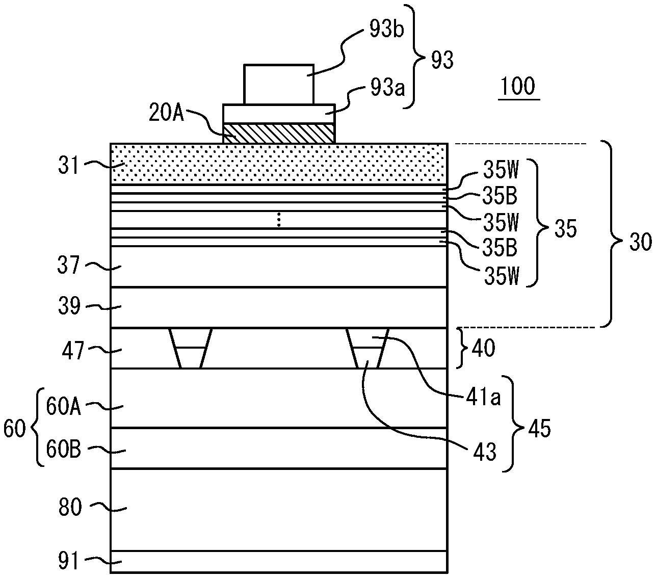
The granted patent US11996496B2 describes a semiconductor light-emitting device designed for efficient light emission in the near-infrared spectrum. The device features a conductive support substrate topped with a reflective metal layer, which enhances light output. A semiconductor laminate, composed of multiple InGaAsP-based III-V group compound semiconductor layers, is layered on the metal. This laminate includes a p-type cladding layer, an active layer structured as a multi-quantum well (MQW) with alternating InGaAsP well and barrier layers, and an n-type cladding layer. An n-type InGaAs contact layer is positioned above the semiconductor laminate, capped with an n-side electrode. The device is engineered to emit light with a center wavelength ranging from 1000 to 2200 nm, and the total thickness of the semiconductor laminate is specified to be between 2 µm and 8 µm. Notably, the In composition ratio of the n-type InGaAs contact layer is defined to be more than 0.532 but not exceeding 0.60.
Further specifications in the claims detail the composition of the n-type InGaAs contact layer, suggesting an optimal In composition ratio of 0.54 or more, while still adhering to the upper limit of 0.60. Additionally, the n-side electrode can be composed of materials such as gold (Au), germanium (Ge), titanium (Ti), and platinum (Pt), which are known for their conductive properties. This patent outlines a novel configuration that may enhance the performance and efficiency of semiconductor light-emitting devices, particularly in applications requiring specific wavelength emissions in the infrared range.
To know more about GlobalData’s detailed insights on Dowa, buy the report here.
Data Insights
From
![]()
The gold standard of business intelligence.
Blending expert knowledge with cutting-edge technology, GlobalData’s unrivalled proprietary data will enable you to decode what’s happening in your market. You can make better informed decisions and gain a future-proof advantage over your competitors.
GlobalData, the leading provider of industry intelligence, provided the underlying data, research, and analysis used to produce this article.
GlobalData Patent Analytics tracks bibliographic data, legal events data, point in time patent ownerships, and backward and forward citations from global patenting offices. Textual analysis and official patent classifications are used to group patents into key thematic areas and link them to specific companies across the world’s largest industries.